Reaserch Background
The exponential growth of data volume in the era of 5G communications and the Internet of Things (IoT) has placed higher demands on the energy consumption, bandwidth and cost of optical communications. In optical communications, silicon optical technology draws on the silicon-based integrated circuit process to integrate optical signal transmission, information loading and demodulation, and data computation on a single chip (i.e., silicon optical chip), resulting in a higher degree of integration, lower power consumption, and lower cost. However, the optoelectronic components in silicon optical chips are limited by the bandgap and mobility of materials such as silicon-germanium, and there is still a lot of room for improvement in the performance of cutoff wavelength, bandwidth, and efficiency, etc. Therefore, it is a hot research topic to search for functional optoelectronic materials and device structures compatible with silicon-optical technology as well as to explore silicon-based optoelectronic heterogeneous integration solutions.
Graphene has unique advantages in integrating with silicon optical chips: no interlayer hanging bonds, which can avoid lattice mismatch and interfacial charge scattering between silicon wafers; high carrier mobility, which has a high upper limit on bandwidth; it can be directly transferred to the silicon optical substrate and is compatible with the silicon-based micro-nanofabrication process, which can satisfy the demand for miniaturization of the device and high-density integration, and so on. However, due to the weak light absorption of single-layer graphene, the current graphene photodetector response is low, which limits its application in high-performance optical communication systems.
To address this problem, the center team, in collaboration with researcher Jianbo Yin in the School of Electronics and Professor Hailin Peng's group in the School of Chemical and Molecular Engineering, has realized the preparation of silicon waveguide-integrated twisted bilayer graphene photodetectors with both high responsivity and bandwidth by using twisted bilayer graphene as a light-absorbing material, which was published in Nature Communications (Nature Commun., 2024) on May 1, 2024, under the title of "Waveguide-integrated twisted bilayer graphene photodetectors" (Nature Commun. 2024, 15, 3688).
Research Content
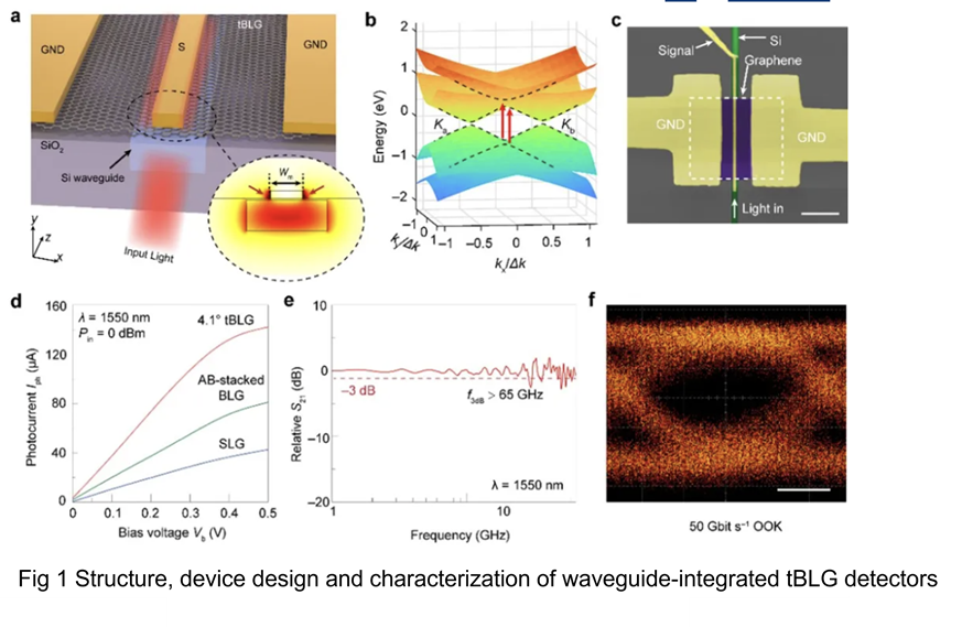
In this work, the joint R&D team integrated twisted bilayer graphene (tBLG) with silicon light. By designing the twisting angle, the energy level difference of the van Hove singularities (vHs) in the tBLG energy bands matches the energy of the photons in the 1,550 nm communication band, which significantly enhances the coupling efficiency with the light; in addition, the linear dispersion relation of the tBLG energy bands near the Dirac point gives it an ultra-high mobility close to that of the single-layer, which ensures the excellent high-frequency performance of the device. Simulation result shows that tBLG has tripled coupling efficiency compared with single-layer graphene, which can effectively shorten the channel length and improve the optical responsivity.

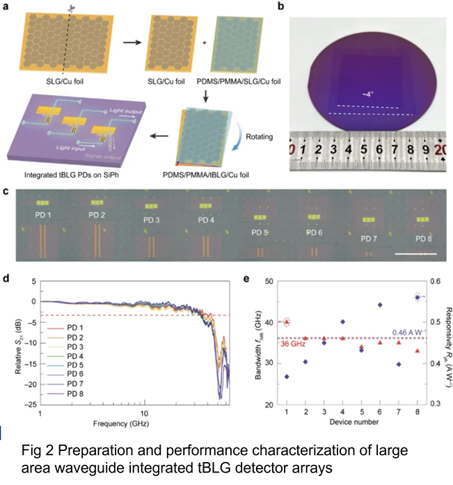
Through theoretical calculations, when the twist angle of the tBLG is 4.1°, the vHs is 0.4 eV away from the Dirac point, which is exactly half of the photon energy of 1,550 nm (0.8 eV), where the optical coupling efficiency is the highest. Combined with the design of the device structure, a high photoresponsivity of up to 0.65 A/W can be realized with a device length of only 8 μm. The average photoresponsivity of multiple devices is 0.54 A/W, which is significantly better than that of single-layer graphene and AB-stacked bilayer graphene devices. The graphene-on-silicon optical device also has a high operating bandwidth in addition to high photoresponsivity, with a 3 dB bandwidth up to 65 GHz (limited by measurement instrumentation), and shows a clear eye-diagram signal in an on-off keying modulation format of 50 Gbit/s. The device has a low power consumption of 0.8 pJ/bit, demonstrating the potential for applications in optical communications. In order to verify the possibility of integrating large-area tBLGs with silicon optics, a large-area waveguide-integrated tBLG photodetector array with a good uniformity performance based on graphene thin-film controllable stacked-layer transfer technique was constructed in this study, which demonstrated a high bandwidth of 36 ± 2 GHz and a high responsivity of 0.46 ± 0.07 A/W, proving that it is possible to integrate tBLGs on a large scale and prepare high-performance optical communication devices. It demonstrates the possibility of large-scale integration of tBLGs and preparation of high-performance optical communication devices.

In this study, the preparation of a photodetector integrated with twisted bilayer graphene and silicon waveguide was realized for the first time, and excellent performance with high responsivity of 0.65 A/W and 3 dB bandwidth of 65 GHz (limited by the measurement equipment) was demonstrated by combining the unique vHs energy band structure of tBLG and the design of device structure. In addition, the preparation of large-area tBLG device arrays and the validation of high responsivity (0.46 ± 0.07 A/W) and bandwidth (36 ± 2 GHz) performances demonstrate the high-quality potential for the preparation of large-scale high-performance optical communication devices by the integration of tBLG with silicon optical heterostructure with vHs and linear dispersive energy-band structure, especially considering the controllable twist angle of tBLG wafer-level growth and the development of graphene wafer-level transfer technology.
Prof. Xingjun Wang of the Center, Prof. Hailin Peng and Researcher Jianbo Yin of the Joint Team are the corresponding authors of the paper, and Luwen Xing, a master student of the Center, is the co-first author of the paper with PhD student Qinci Wu, Postdoctoral Fellow Jun Qian, and PhD student Yuechen Wang of the Joint Team. Other co-authors include Ziyi Wei, a graduated master student of the Center; Zhongfan Liu, academician and Hongtao Liu, associate researcher of the School of Chemical and Molecular Engineering; Xin Gao and Yurui Li, doctoral students of the Institute of Frontier Interdisciplinary Research. This research work was funded by the Ministry of Science and Technology, the National Natural Science Foundation of China and other institutions and programs, and supported by the Instrumentation Platform of Molecular Materials and Nanofabrication Laboratory, School of Chemical and Molecular Engineering, Peking University, and the State Key Laboratory of Regional Optical Fiber Communication Network and Novel Optical Communication System, School of Electronics, Peking University.
Link to the original paper:
https://www.nature.com/articles/s41467-024-47925-x

